Tue 19 June 2007 |
| More spacer creation and then assembly. | 
|
| The finished product - only a single LED lit for this photo, but you can see the final 'look'. Now I need to work on the driver / control board and think about mounting. | 
|
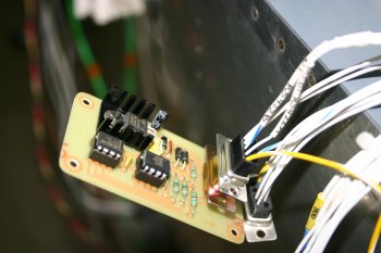
| Next was the FADEC RS422/RS232 PCB. This is a simple single sided board, and a bit smaller than the others. | 
|
| After drilling and soldering up - has dual supplies, a fixed voltage regulator and a couple of ICs. | 
|
| This was probably the most challenging of the PCB designs - the FADEC SBC RS422 to EIS RS232 protocol conversion.
Although it ended up being a fairly simple board in the end, the research and lack of experience with this type of design / components was difficult.
The comercial options are about US$80 and have problems with power supply (they use the RS232 DTS/RTS lines for power - which we don't have).
However it worked first time and seems to work well - the success was really quite sweet. | 
|


