PCBs |
|
| | 
|
| | 
|
| | 
|
| | 
|
| | 
|
| | 
|
| | 
|
| | 
|
| | 
|
|
| | 
|
| | 
|
| | 
|
| | 
|
| | 
|
| | 
|
|
| Also spent another couple of hours re-doing the LED annunciator PCB layout. I think I have a workable solution using a double sided board. | |
|
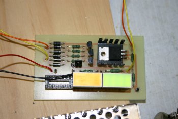
| With a slow day on other things I spent a bit more thought and design work on some of the PCB designs. Another test board was laid out to confirm the voltage regulator / LED balast resistors and I started the fabrication process. | 
|
|
| Only a few hours with other commitments - I did finish making the test PCB - the dimming levels work well and the small bit of custom logic seems to work ok. Just a stepping stone for the bigger solution. | 
|
|
| Getting real cold outside and am in a low productivity mode at the moment - started the dual layer LED board - this is the 3x2 matrix for the critical indicators - P1 side. | 
|
| The 'vias' between top and bottom layers are just small wire links - seems to work ok although the alignment is very fiddly. | 
|
| Finished board, ready for wiring and the additional LEDs. LEDs are currently on order from RS components (deliveries from Auckland, Sydney and London!) and the wire I got from Stein last week. | 
|
|
| Laid out and twisted the multi core cable bundle for the LED panels. Dog comb worked well for keeping the tangling to a minimum. | 
|
| Wired up for testing - looks good. Currently using white paper as the mask, provides a good dead facing solution, but intensity of colour is a little less than I would like. More research / would like to try a translucent mylar if possible. | 
|
| The finished 3x2 board from the side, you can see the PCB, carriers, LEDs, standoffs, paper mask, plexi-glass sandwich. | 
|
|
| I decided a temperature control soldering iron was needed - so another chance to buy more tools..... | 
|
| Then onto the 3x3 LED board - a few extra photos, one for each of the steps. | 
|
| Top and bottom accete masks. | 
|
| Attached to glass plate. The actual laser 'soot' is on the bottom surface and therefore in contact with the PCB board. | 
|
| Expose to light (UV I think is the important bit) - normally for about 14 mins, repeat on second side. | 
|
| Develop the mask - the white spacers are to help prevent scratching of the lower surface. | 
|
| Etch in ferric chloride for ~15 mins and you get a base board | 
|
| Then lots of drilling, mixture of .6mm, .75mm and #60 and #57 used for the components, #33 for the mounting locations. Via's soldered first, then the DIL sockets. | 
|
| Finished board ready for LEDs - Forward surface / back of board) | 
|
| Aft surface / front of board. | 
|
| Then 4 spacers, #4 thread through the center and parted to the right length to keep the LEDs up tight against the plexi-glass surface. | 
|
|
| More spacer creation and then assembly. | 
|
| The finished product - only a single LED lit for this photo, but you can see the final 'look'. Now I need to work on the driver / control board and think about mounting. | 
|
| Next was the FADEC RS422/RS232 PCB. This is a simple single sided board, and a bit smaller than the others. | 
|
| After drilling and soldering up - has dual supplies, a fixed voltage regulator and a couple of ICs. | 
|
|
| PCB design and research. Also looking at the AVR microprocessor chipset | |
|
| More chip research but also design / layout work is actually productive progress! | |
|
| Dual speed, dual trim PCB boards - expose, develop and etch step | 
|
| Drill, populate and solder. Seems to be about a 4-6 hours process for each PCB - that is after the multiple hours doing the design and track layout work. | 
|
|
| Finally back to plane work - only a couple of hours, but got the annunciator control board masked, developed and etched. | 
|
|
| Annunciator PCB drilling / layout. | 
|
| Worked round the smaller (cheaper) resistors and diodes then the connectors, voltage regulators etc. All finished after a few hours. Testing was limited but seems to be working fine. | 
|
|
| Got the mouser order - including the new AVR microprocessor chips. Still cold / grotty outside so started playing. Took it one step at a time, got a basic power supply, reset line and led connected. | 
|
|
| The basic "hello world" of embedded system now works - it is a simple flashing LED! | 
|
|
| More serious AVR work - starting looking at the SD card interface and thinking about coding for FAT file systems. Short version of multiple days work - I was struggling to understand frequency generation settings, lots of people provided information, but it took about a week of frustration and support from the factory to identify my mistake and the solution. All rather frustrating but part of the learning process of a new technology. | 
|
|
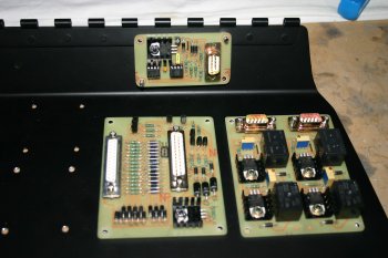
| This is the planned layout of the new PCB boards on the RHS drop down panel. Annunciator control, dual trim control and RS422/232 convertor at the top. | 
|
| Spent most of the day turning up threaded spacers for the PCB. Slow but the right solution for a neat finish. | 
|
|
| The finished layout with spacers. The two left locations are for the CO detector and flap control board. | 
|
|
| More PCB fabrication - this is a power supply for the ANR headset I have on order. It is a isolated 9V DC supply. | 
|
| Very simply, when you can find a supplier of the C & D Technologies componenets. | 
|
|
| Also made a switch mode power supply which can handle up to 3A. This is planned for a DV video camera. | 
|
|
| More PCB fabrication - UART datalogger - this is double sided which complicates things a little. | 
|
| The etch was a little problematic, but the alignment came out really well. I tinned the surface mount pads and fixed a problem track. Then started the via and component drilling - a slow process. | 
|
|
| Finished drilling and soldered up the data logger. The surface mount card adapter actually went well in the end - a nice surprise. | 
|
|
| Mounted and testing the ANR power supply. | 
|
|
| We've been chasing a couple of minor electrical bugs for a while - finally managed to work out the issue on the EIS warning light. Simple pull up resistor fix needed. | 
|


